In industrial inspection, medical imaging, wireless receiving front-ends, and high-performance data acquisition systems, analog signal chains face a common challenge: increasing front-end signal bandwidth, expanding channel counts, and growing data throughput demands on the main controller, all while maintaining power efficiency, thermal design, and compact size. For ADC selection, focusing solely on "sampling rate" or "resolution" is insufficient. The true determinant of project delivery quality lies in the "system-level implementability of parameters."
The CD96AD53 from ChisynV is specifically designed for multi-channel high-speed acquisition applications. Featuring 4 channels, 16-bit resolution, and a maximum sampling rate of 125 MSPS, it operates on 1.8V power and utilizes LVDS serial digital interface. Capable of functioning across an industrial temperature range of-40°C to +85°C, the device is packaged in a QFN-48 format. Its pin-to-pin compatibility with the ADI AD9653 makes it the preferred domestic alternative for industrial-grade scenarios.
Core Performance
The CD96AD53 features 16-bit resolution and 650MHz full-power analog bandwidth, supporting a maximum sampling rate of 125MSPS for precise wide-band signal acquisition. Its configurable reference voltage delivers 9.7MHz input signal-to-noise ratio (SNR) of 75dBFS and 91dBc spurious-free dynamic range (SFDR) at VREF=1.0V, with SNR improvement to 77dBFS at VREF=1.3V. Core specifications including ±0.6LSB differential nonlinearity (DNL) and ±5.0LSB integral nonlinearity (INL) significantly reduce conversion distortion, meeting industrial-grade requirements for signal acquisition resolution and fidelity without additional compensation circuits. Additionally, its dual-tone intermodulation distortion of-90dBc and conventional crosstalk suppression of-91dB effectively resist industrial environmental interference, ensuring stable signal acquisition.
The device features a single 1.8V power supply, with analog/digital/driver power supplies supporting a wide voltage range of 1.75V to 1.9V. In 125MHz mode, each channel consumes ≤195mW, while the typical power consumption is <14mW when all channels are disabled and drops to 2mW in power-saving mode. It supports independent channel shutdown and standby modes, flexibly meeting diverse energy requirements and significantly reducing overall system power consumption. The SPI serial port enables full-chip and independent channel power management, multi-chip synchronization, 1-8x clock frequency division, and customizable test mode configurations.
The CD96AD53 supports an industrial temperature range of-40°C to +85°C, featuring a QFN-48 package. It supports LVPECL/CMOS/LVDS-compatible sampling clocks, with LVDS serial output compliant with ANSI-644 standards by default. The device also offers IEEE low-power mode switching, allowing flexible configuration of output formats, drive strength, and termination resistances to meet diverse backend processing circuit interface requirements. As a pin-to-pin compatible variant of the ADI AD9653, it enables zero-change design replacement, effectively mitigating overseas component supply chain risks and significantly reducing R&D and time costs for domestic substitution.
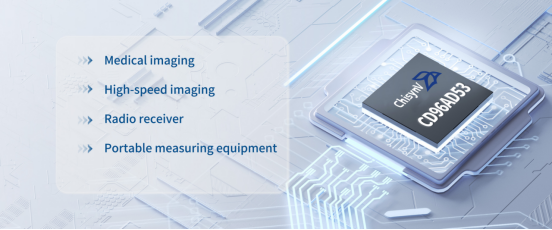
scenario value
In medical imaging, high signal-to-noise ratio (SNR) and low nonlinear distortion ensure image resolution for ultrasound and endoscopic devices, while the wide temperature range accommodates the operational requirements of medical equipment.
In high-speed imaging scenarios, the 125MSPS sampling rate and 650MHz bandwidth enable precise capture of fast-moving target signals, while the independent channel shutdown function accommodates multi-angle synchronous acquisition requirements.
In radio receiver applications, the wideband acquisition capability and multi-chip synchronization function perfectly align with the orthogonal/diverse reception architecture, thereby enhancing signal reception efficiency.
In the field of portable testing devices, low-power design and compact packaging enable optimized product form and extended battery life while maintaining high acquisition accuracy.